Analog IC design does not end when the schematic meets its specifications. The circuit must survive its translation into geometry: matched devices need matched environments, high-impedance nodes need short and quiet routes, power paths need low resistance, and every shape must satisfy the process design rules. This tutorial walks through that complete flow using a Miller-compensated two-stage CMOS operational amplifier, followed by a non-inverting gain-of-two application with pads and ESD protection.
The emphasis is not on one particular PDK. Instead, the goal is to show a reusable way to move from specifications to transistor sizing, pre-layout verification, matching-aware layout, DRC/LVS/PEX, and post-layout sign-off.
1. Define the design target
The example uses a 1.8 V, 0.18 µm CMOS process. The open-loop amplifier is designed around the following targets:
| Metric | Target | Why it matters |
|---|---|---|
| DC open-loop gain | ≥ 80 dB | Reduces closed-loop gain error |
| Unity-gain frequency | ≥ 1 MHz | Sets the useful closed-loop bandwidth |
| Typical phase margin | ≥ 60° | Provides a well-damped transient response |
| Corner phase margin | ≥ 45° | Maintains stability across PVT variation |
| Power | As low as practical | Constrains branch currents and device sizes |
A useful habit is to keep the specification table visible throughout the project. Every sizing choice, simulation, and layout compromise should map back to one or more rows in this table.
2. Choose a topology that matches the problem
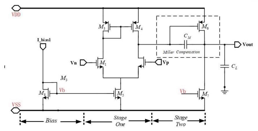
A classic two-stage architecture is a strong starting point when high DC gain and a reasonably large output swing are required:
- First stage: an NMOS differential pair (M1 and M2) with a PMOS current-mirror load (M3 and M4). This stage provides differential-to-single-ended conversion and much of the voltage gain.
- Second stage: a PMOS common-source device (M6) with an NMOS current-source load (M7). It adds gain and improves output swing.
- Bias network: a diode-connected NMOS reference device (M8) biases the first-stage tail source M5 and the second-stage load M7.
- Frequency compensation: a Miller capacitor, Cc, connects the first-stage output to the amplifier output and separates the dominant and non-dominant poles.
At zero differential input, the tail current divides equally:
The topology is intentionally simple. Simplicity helps both electrically and physically: fewer internal nodes reduce parasitic uncertainty, and a regular device structure is easier to match in layout.
3. Establish the current plan before sizing devices
Start with a 10 µA reference current. Mirror ratios then establish the branch currents:
- M8 carries 10 µA.
- M5 uses a 2× ratio and supplies 20 µA to the input pair, or approximately 10 µA per side at zero differential input.
- M7 uses an 8× ratio and biases the second stage at approximately 80 µA.
The second stage deliberately receives more current than either half of the input stage. Its higher transconductance pushes the non-dominant pole upward and gives the output node more drive capability.
The final device set used in this case study is:
| Device | Type | Unit W/L (µm/µm) | Multiplier | Approx. current |
|---|---|---|---|---|
| M1, M2 | NMOS input pair | 2.25/1 | 2 | 10 µA each |
| M3, M4 | PMOS mirror load | 9/1 | 1 | 10 µA each |
| M5 | NMOS tail source | 4.5/1 | 2 | 20 µA |
| M6 | PMOS second stage | 4.5/1 | 16 | 80 µA |
| M7 | NMOS second-stage load | 4.5/1 | 8 | 80 µA |
| M8 | NMOS bias reference | 4.5/1 | 1 | 10 µA |
| Cc | MIM capacitor | — | — | 4.5 pF |
Longer-than-minimum channel lengths are useful here because they improve output resistance, intrinsic gain, and matching. The cost is area and parasitic capacitance, so the choice should always be verified in simulation.
4. Use first-order equations to guide simulation
For a long-channel MOS device in saturation, a useful first-order transconductance estimate is:
For a Miller-compensated two-stage op-amp, the gain-bandwidth product is approximately:
With an input-device transconductance near 101 µS and Cc = 4.5 pF, the first-order estimate is about 3.57 MHz. This clears the 1 MHz requirement with margin. The simulated result is higher because the compact hand calculation ignores several second-order effects.
The second-stage transconductance is approximately 792 µS—almost eight times gm1:
That ratio is helpful because the non-dominant pole roughly tracks the second-stage transconductance divided by its load capacitance:
A stronger second stage therefore makes it easier to maintain phase margin after compensation.
These equations are not substitutes for transistor-level simulation. Their job is to establish a sensible starting point and to explain why a later simulation result moves in a particular direction.
5. Verify the schematic before drawing layout
Run the following checks before opening the layout editor:
- DC operating point: confirm every MOS device is in saturation over the intended common-mode and output ranges.
- Open-loop AC or stability analysis: measure low-frequency gain, UGF, and phase margin.
- PVT corners: include slow/high-temperature/low-voltage and fast/low-temperature/high-voltage extremes.
- Closed-loop transient tests: check settling, distortion, and slew rate at the intended noise gain.
- Noise: identify which devices dominate the input-referred noise.
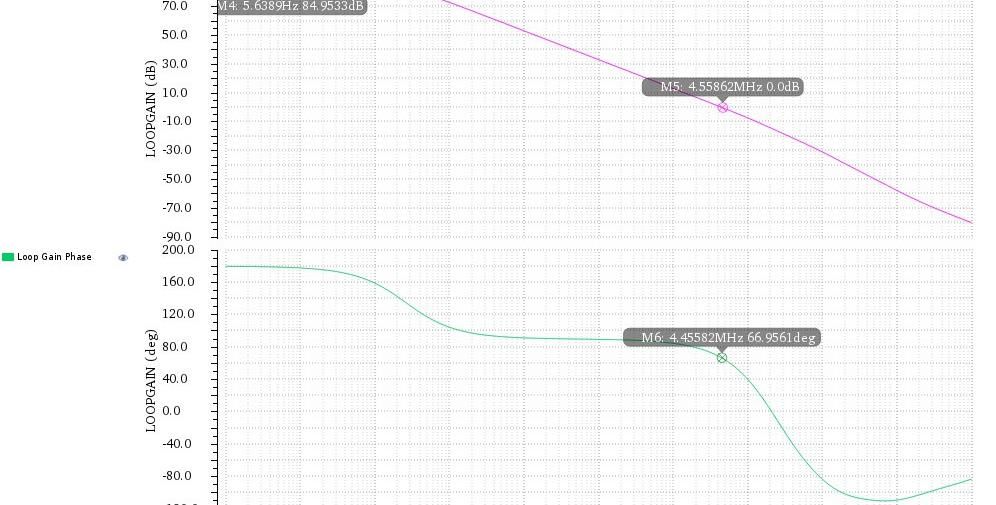
At the typical corner, the open-loop simulation produced 84.95 dB of gain, a 4.56 MHz UGF, and 66.44° of phase margin. The slow corner reached 3.79 MHz with 67.22°, while the fast corner reached 5.83 MHz with 65.43°. All three cases met the target.
For the closed-loop DC operating point, the measured total current was about 111.1 µA, giving:
6. Translate electrical intent into a floorplan
Layout should begin with a placement plan, not with routing. Group devices by matching requirement and signal sensitivity:
6.1 Differential pair
Split M1 and M2 into equal fingers and use a two-dimensional common-centroid pattern such as:
D  M1  M2  D
D  M2  M1  D
This arrangement averages both horizontal and vertical process gradients. Keep the source connections, gate routes, drain loading, contacts, and surrounding dummy environment as symmetric as possible. Common-centroid placement does not help if the routing destroys the symmetry.
6.2 PMOS mirror and second-stage device
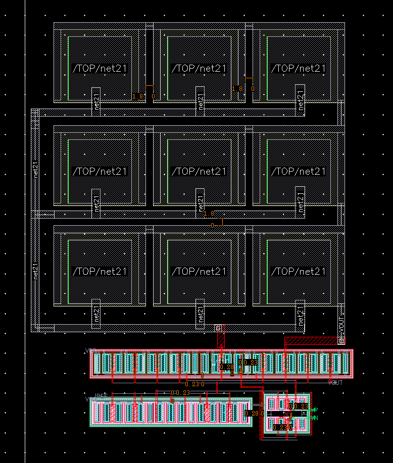
Place the matched PMOS load devices near the center of a shared well. An A-B-B-A arrangement gives M3 and M4 a similar neighborhood. The large M6 device can be split into two equal groups and placed symmetrically around the matched pair so that its area does not force a one-sided floorplan.
6.3 NMOS current mirrors
Place the reference device M8 centrally, put the two M5 halves close to it, and distribute the M7 fingers symmetrically toward the outside. Equalize gate routing from the bias node and use the same contact style on every mirror member.
6.4 Compensation capacitor
Keep the MIM capacitor away from noisy digital or large-swing routes. More importantly, keep both of its connections short: one terminal touches the sensitive first-stage output, while the other connects to the amplifier output. Excess parasitic capacitance on the first-stage node directly changes the pole-zero locations.
7. Route in order of sensitivity
A practical routing order is:
- Matched differential and mirror connections.
- The first-stage high-impedance output and both compensation-capacitor terminals.
- Bias lines.
- Output path.
- Power and ground.
Use wider metal and dense via arrays for supply and output paths. Keep high-impedance routes short, avoid running them parallel to large-swing nets, and add shielding only when the shield can be tied to a genuinely quiet node. A poorly chosen shield can add more capacitance than the coupling it removes.
8. Close the DRC–LVS–PEX loop
8.1 DRC is more than a final checkbox
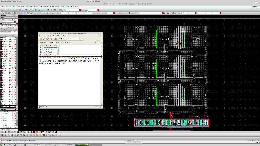
Run DRC incrementally. In this layout, two representative violations were minimum Metal 1 spacing in a dense local route and insufficient spacing on the top metal near a power or capacitor connection. Both were fixed by replanning the route rather than applying a cosmetic patch.
When a fix changes symmetry, immediately check its matched counterpart. A geometrically legal asymmetry can still create an analog error.
8.2 LVS checks connectivity, not performance
A clean LVS result confirms that layout and schematic have the same devices and nets. It does not confirm matching quality, current density, antenna robustness, or stability. Treat LVS as one layer of evidence, not as the definition of a good layout.
8.3 PEX exposes naming and parasitic mistakes
After LVS, extract resistance and capacitance, including coupling capacitance. A subtle but common failure is inconsistent terminal naming. In this case, mixed-case input labels in the schematic did not match uppercase layout pins. Renaming the schematic pins consistently allowed the extracted view to netlist correctly.
This is a useful debugging rule: when PEX reports a netlist mismatch after LVS is clean, inspect view selection, terminal direction, bus syntax, hierarchy, and case sensitivity before redrawing geometry.
9. Compare pre-layout and post-layout results
Post-layout simulation should use the same testbenches, measurements, corners, and plotting conventions as pre-layout simulation. Otherwise, the comparison is ambiguous.
| Metric | Pre-layout | Post-layout | Change |
|---|---|---|---|
| Open-loop gain | 84.95 dB | 84.92 dB | −0.03 dB |
| Unity-gain frequency | 4.56 MHz | 4.46 MHz | −0.10 MHz |
| Phase margin | 66.44° | 66.37° | −0.07° |
The small UGF reduction is expected: routing adds capacitance to internal high-impedance nodes. The important result is not that the values are identical, but that the degradation is small, explainable, and still leaves comfortable specification margin.
10. Turn the op-amp into a practical gain-of-two block
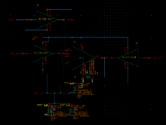
To verify the amplifier in a realistic closed-loop configuration, connect it as a non-inverting amplifier with equal feedback and ground resistors:
Use equal resistor geometry and place the two functional resistors in the same array. A simple pattern is:
Dummy Rf Rg DummyThe dummies make the etch and stress environment of the two functional resistors more similar. Ratio accuracy matters more than absolute resistance because the closed-loop gain depends on Rf/Rg.
The 10 kΩ value is also a compromise between output loading and resistor noise. The resistor’s thermal-noise voltage density is:
Very small resistors unnecessarily load the output, while very large resistors increase thermal noise and create lower-frequency poles with parasitic capacitance.
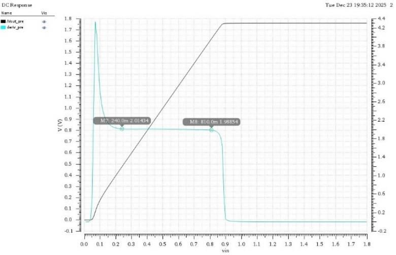
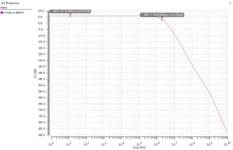
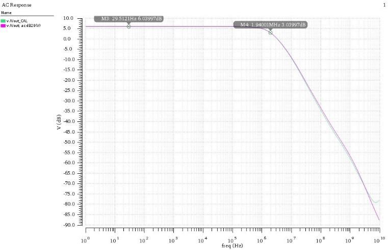
The pre-layout closed-loop simulation produced 6.038 dB of gain, very close to the ideal 6.02 dB, with a −3 dB bandwidth of 1.979 MHz. A DC sweep identified approximately 0.6 V as a useful common-mode bias point for the largest linear output range.
11. Add pads, ESD, and top-level routing
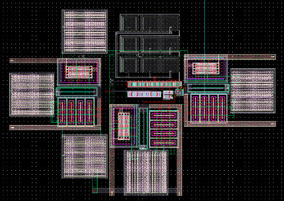
The top-level layout integrates the op-amp core, feedback network, I/O protection, and pads. Place the sensitive core and feedback resistors near the center. Arrange signal and supply pads around the perimeter, and provide short, low-impedance discharge paths from each ESD cell to the supply rails.
A wide power ring and generous via arrays reduce both normal IR drop and transient ESD impedance. Avoid routing a protected signal through a long narrow path after the clamp; that inductive and resistive segment can defeat the intended protection during a fast event.
12. Measure the cost of pads and extraction
After extracting the complete top level, compare it with the schematic-level application:
| Metric | Pre-layout | Post-layout | Interpretation |
|---|---|---|---|
| Closed-loop gain | 6.038 dB | 6.040 dB | Resistor ratio preserved |
| −3 dB bandwidth | 1.979 MHz | 1.940 MHz | About 2% reduction |
| Slew rate | 1.398 V/µs | 1.377 V/µs | Small parasitic penalty |
| Integrated input-referred noise | 96.57 µV RMS | 96.43 µV RMS | Essentially unchanged |
The noise report also illustrates how schematic abstractions map to physical devices. A transistor represented with a multiplier of two can appear after extraction as two parallel finger devices. Their individual noise contributions may be reported separately, but their sum should remain close to the original device contribution. This is expected behavior, not a new noise source.
13. A reusable sign-off checklist
- All critical devices remain in the intended operating region across PVT.
- Typical and worst-case gain, bandwidth, phase margin, power, noise, and slew rate meet the specification.
- Matched devices have equal geometry, orientation, contacts, routing, and edge environment.
- High-impedance nodes are short and isolated from large-swing routes.
- Supply and ESD paths use adequate width and via density.
- DRC is clean at both block and top level.
- LVS is clean with the intended hierarchy and device parameters.
- PEX includes the required resistance, capacitance, and coupling models.
- Post-layout tests reuse the pre-layout benches and measurement definitions.
- Every performance shift has a plausible physical explanation and sufficient remaining margin.
Conclusion
The central lesson of analog layout is that geometry is part of the circuit. Common-centroid placement, dummies, symmetric routing, careful pole-node wiring, ratio-matched resistors, and low-impedance pad protection are not aesthetic choices—they determine whether the schematic behavior survives fabrication.
In this example, the extracted open-loop UGF changed from 4.56 MHz to 4.46 MHz, and the complete gain-of-two block lost less than 2% of its bandwidth after pads and ESD were included. Those small, predictable shifts are the reward for treating layout constraints as part of the electrical design from the beginning.