A compact radar antenna has two jobs that can work against each other: radiate efficiently toward the scene, and keep the transmitter from coupling directly into the receivers. A wide impedance bandwidth alone does not solve the second problem. The package, feed structures, polarization, and spacing all influence the leakage paths.
This walkthrough develops a simulated 60 GHz antenna-in-package (AiP) array with one transmit element and three receive elements. It combines an L-probe-fed patch element with increased spacing, orthogonal transmit/receive polarization, and an L-shaped via fence. The focus is the design process: establish a baseline, change one mechanism at a time, and verify matching, coupling, and radiation together.
Scope: this walkthrough presents electromagnetic simulation results and a reusable design method. Fabricated-module measurements and a complete manufacturing specification are outside its scope.
1. Define the bandwidth and isolation targets
The intended radar band is 57–64 GHz. The antenna element is based on a published design with a wider simulated matching band of 56–67 GHz, providing useful frequency margin. Use port 1 for Tx and ports 2–4 for Rx when interpreting the coupling plots.
| Quantity | Design objective | What to check |
|---|---|---|
| Port matching | Sii < −10 dB | All four ports over the intended band |
| Tx–Rx isolation | > 30 dB | All three transmit-to-receive paths |
| Rx–Rx isolation | > 20 dB | Every receive-port pair |
| Element gain | > 5 dBi | Useful broadside radiation without a split main beam |
| Architecture | 1 Tx + 3 Rx | A compact 2 × 2 physical arrangement |
Be precise about the sign convention. A coupling trace of −30 dB corresponds to 30 dB of isolation, not “negative isolation.” With the other ports matched:
At 60 GHz, the free-space wavelength is approximately 5 mm. That makes millimeter-scale layout changes electrically significant:
For an ideal FMCW radar, the swept signal bandwidth sets range resolution. A 7 GHz sweep gives approximately 2.14 cm; an 11 GHz sweep gives approximately 1.36 cm. Antenna bandwidth makes such a sweep possible, but does not by itself establish the usable bandwidth of the complete radar.
2. Start from the referenced L-probe-fed element
The antenna element is adapted from “Wideband L-Probe Fed Antenna-in-Package Module for Millimeter-Wave Radar”, presented at the 2024 IEEE Conference on Antenna Measurements and Applications (CAMA). The element topology and baseline bandwidth come from that reference; the 1T3R arrangement and hybrid decoupling study discussed here are the subsequent project work.
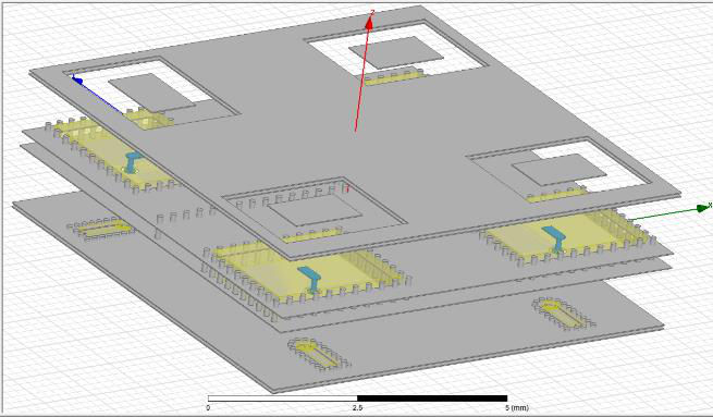
The referenced element has three main parts: a rectangular radiating patch, an L-shaped feed probe, and a metal-backed cavity. Its HDI stack-up uses five dielectric layers and six metal layers, with relative permittivity 3.5, 250 μm core layers, 50 μm prepreg layers, and 18 μm metallization. These are reference-design parameters, not a complete manufacturing specification for this array.
The vertical probe contributes inductive reactance. Its horizontal arm couples capacitively to the patch, providing another tuning degree of freedom. A useful first-order picture is:
This equivalent circuit explains the tuning direction; it does not replace a full-wave model of the coupled patch and probe. Sweep patch dimensions, horizontal probe length, and probe-to-patch separation while watching the entire matching band. The cavity and its via walls also shape substrate fields and back radiation.
The reference reports a 56–67 GHz simulated impedance bandwidth. Using the arithmetic band center gives:
Do not confuse the two rotation strategies: the reference explores rotating both antennas by 45° relative to their layout; this project rotates the Tx element by 90° relative to the Rx elements to introduce orthogonal polarization.
3. Build the 1T3R layout
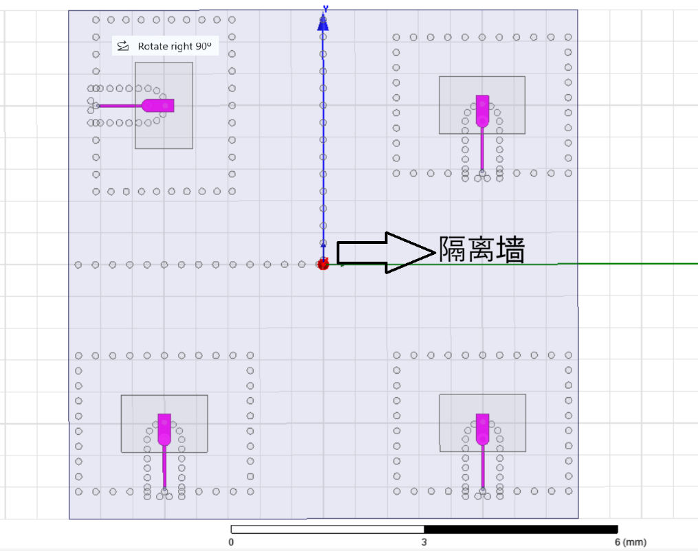
Arrange the elements in a 2 × 2 footprint. In the project development, the element spacing increased from 3.0 mm to 5.0 mm before adding polarization and via-fence decoupling. At 60 GHz those distances are approximately 0.6λ0 and 1.0λ0. More spacing changes the coupling environment, but also consumes package area.
Rotate the Tx patch and feed together by 90°; retain the original orientation for all three Rx elements. Then place an L-shaped metal via fence between the Tx region and its adjacent receive regions. Preserve electrical connections to the intended metal planes, and check that the fence does not intersect feeds or disturb the individual cavity boundaries.
4. Assign a job to each decoupling mechanism
Spacing changes the field strength and phase seen by neighboring elements. Keep it fixed when comparing the other two mechanisms, otherwise an apparent improvement cannot be attributed cleanly.
Orthogonal polarization reduces coupling between differently oriented fields. For two ideal linearly polarized plane waves, polarization overlap follows:
The ideal overlap is zero at 90°, but a compact packaged array is not a pair of ideal plane waves. Near fields, finite cross-polarization, shared grounds, and substrate paths leave residual coupling. Orthogonal Tx/Rx polarization can also reduce the desired echo from polarization-preserving targets, so port isolation must eventually be checked against the radar link budget and target scattering behavior.
The via fence modifies the substrate-field paths and acts approximately as a conducting boundary. Its effectiveness depends on via diameter, pitch, height, plane connections, and placement. A simple pitch smaller than half a wavelength is not sufficient to guarantee a good wall: use the relevant dielectric or guided wavelength, account for the gap between vias, and confirm the result with full-wave fields and S-parameters.
The mechanisms interact. Adding a fence can improve one frequency region while introducing ripple elsewhere. Optimize the worst-case response across the band rather than the depth of one attractive isolation notch.
5. Set up a controlled simulation sequence
Use the following workflow to compare the decoupling mechanisms in a full-wave solver:
- Validate one element. Include the stack-up, finite conductivity, dielectric loss, feed, and cavity. Establish matching and broadside radiation before building the array.
- Create the spaced array. Start with the same element geometry and a fixed 5.0 mm spacing. Use consistent port definitions and reference planes.
- Compare polarization. Evaluate co-polarized and orthogonal arrangements without the added fence. Keep the remaining geometry and solver settings fixed.
- Add the fence. Compare the orthogonal arrangement with and without the L-shaped via fence. Inspect substrate fields as well as port coupling.
- Check every port. Excite one port at a time with the others matched. Evaluate all four reflections, three Tx–Rx paths, and three Rx–Rx pairs.
- Resolve narrow resonances. Sweep 50–70 GHz for context, refine the frequency sampling near peaks, and verify mesh convergence around probes, gaps, and vias. Repeat far-field checks near the band edges and center.
Record the mesh, loss models, and convergence settings so that each comparison can be reproduced.
6. Read the matching and coupling results
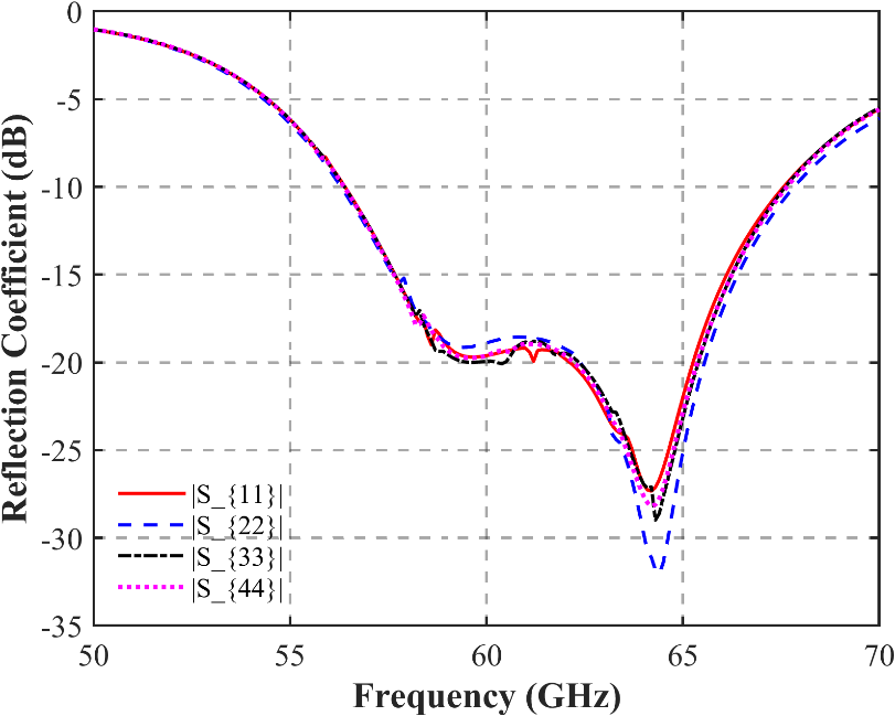
The four reflection curves track closely. They show a broad matched region and a deeper minimum near 64 GHz. Extract each threshold crossing from numerical data before reporting exact bandwidth: the image supports an approximate band, not sub-gigahertz endpoint precision.
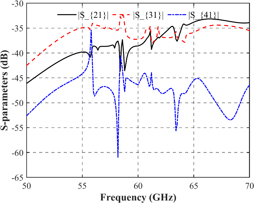
The displayed Tx–Rx traces remain below −30 dB, supporting the 30 dB objective. Local coupling peaks approach −32 dB, so the plots do not establish a strict 33 dB minimum isolation at every frequency.
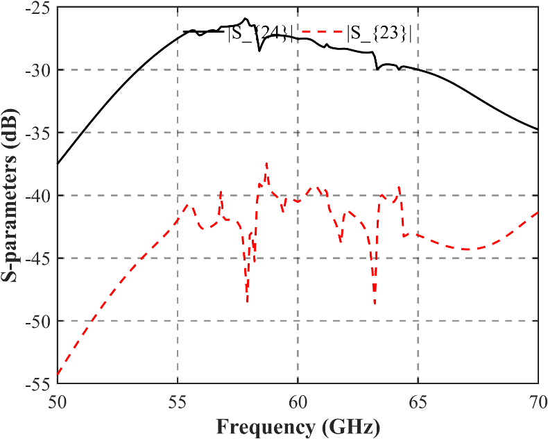
The shown receive-port paths exceed the 20 dB isolation objective. However, this figure does not show every Rx–Rx pair in the final layout. Do not assume the missing path is identical unless symmetry or the full S-matrix establishes it.
7. Separate polarization and fence effects
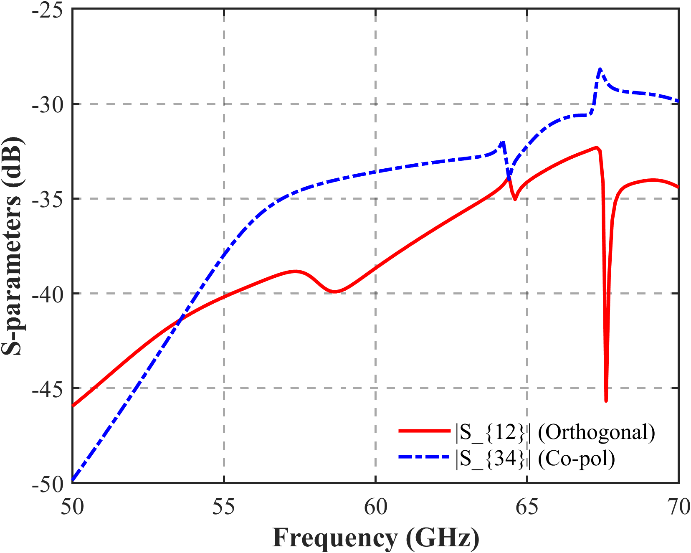
Over much of the intended band, the orthogonal pair has lower coupling, with roughly 5 dB improvement in several regions. Near 67 GHz the co-polarized trace approaches −28 dB. The curves cross at the low end of the wider sweep, so polarization is not uniformly better at every plotted frequency. Also, this comparison uses different port pairs; a stricter attribution experiment would rotate the same pair while holding all other geometry fixed.
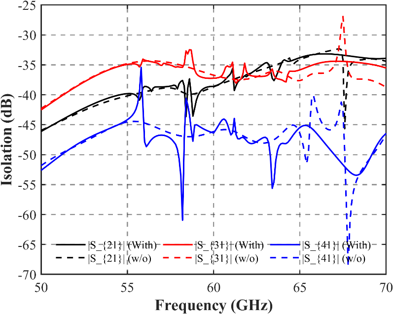
The no-fence red trace rises to about −27 dB near 67.5 GHz, outside the intended 57–64 GHz radar band and just above the reference matching band. The fence suppresses this high-frequency deterioration. That is useful evidence of additional margin, but should not be described as a failure inside the intended band. Elsewhere, ripple and notches move in both directions: the benefit is frequency-dependent.
8. Check radiation before accepting the design
Low coupling is not enough if the antenna loses useful gain or sends energy away from the target. The simulation results give approximate peak gains of 5.8 dBi for Tx and 5.9 dBi for Rx, with broadside main beams and a front-to-back ratio greater than 20 dB. The polar plots below illustrate the radiation shape; their frequency and trace labels are insufficient to independently verify each numerical value.
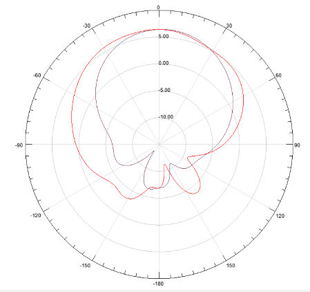
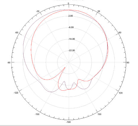
For a final design review, export realized gain, radiation efficiency, co- and cross-polarized cuts, and front-to-back ratio for every active port at clearly stated frequencies. Follow this with a radar-level test that includes the target’s polarization response. An isolation improvement is only useful if the desired echo remains detectable.
9. What this design demonstrates
The most reusable lesson is to treat antenna isolation as a combination of paths. Spacing changes the interaction geometry; polarization reduces some direct coupling; the via fence reshapes substrate and near-field paths. The simulations support a wide matched band, Tx–Rx isolation above the 30 dB design objective in the displayed sweep, and approximately 26 dB or better isolation for the receive pairs shown.
Before fabrication, complete the dimensioned stack-up and feed definition, verify the full S-matrix with converged numerical data, sweep manufacturing tolerances, and account for packaging and material losses. The present figures provide a useful design study, not measured proof of radar sensitivity or a guarantee across process variations.
Antenna-element reference
Wideband L-Probe Fed Antenna-in-Package Module for Millimeter-Wave Radar. 2024 IEEE Conference on Antenna Measurements and Applications (CAMA), IEEE, 2024. DOI: 10.1109/CAMA62287.2024.10986250.
The referenced work provides the antenna-element starting point for this design.