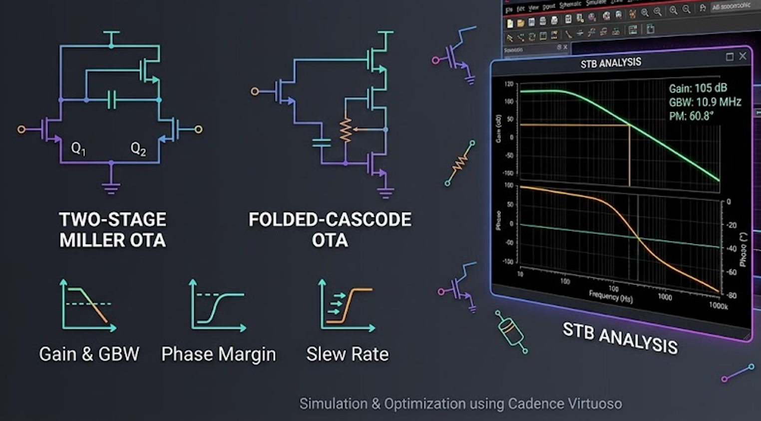

In this post, we will walk through the systematic design and simulation of Operational Transconductance Amplifiers (OTAs) using the GlobalFoundries BCDlite process. We will cover the topology, working principles, and frequency compensation techniques for two classic architectures: the Two-Stage Miller Compensated OTA and the Folded-Cascode OTA.
By the end of this guide, you will understand how to translate circuit specifications (Gain, Bandwidth, Slew Rate) into small-signal parameters (, ), determine transistor dimensions, and verify your design using Cadence Virtuoso.
Part 1: Two-Stage Miller Compensated OTA Design
Our first design is a two-stage Miller compensated OTA featuring an NMOS differential input stage and a PMOS common-source second stage. We use a Miller capacitor () for frequency compensation and a series nulling resistor () to eliminate the effect of the right-half-plane (RHP) zero.
1.1 Slew Rate (SR) and Load Driving Capability
We start by determining the tail current and compensation capacitor based on the Slew Rate (SR) and load capacitance requirements.
- Design Target:
- Design Process:
For a two-stage OTA, the Slew Rate is typically limited by the charging/discharging speed of the Miller capacitor (limited by the first-stage tail current) or the load capacitor (limited by the second-stage output current). The empirical formula is:Considering Phase Margin (PM) requirements, we usually select . Given a load , and ensuring isn’t too small to avoid parasitic effects, we select:
Final Value: . Substituting this into the SR formula to find the required tail current ():To leave enough margin and improve bandwidth, we design the tail current to be significantly larger than the theoretical minimum. We use a reference current and a current mirror ratio of 1:6, resulting in a first-stage tail current of . This yields a theoretical SR of , far exceeding the target.
1.2 Determining Input Transconductance ()
- Design Target: Gain-Bandwidth Product ()
- Design Process:
The Unity Gain Bandwidth (UGF or GBW) is approximately:
Working backwards from the requirement:
With a single-branch current and NMOS process parameter , we use the transconductance formula to size the input transistors (M1, M2). To maximize gain, we choose a large channel length: and ().
The estimated is , yielding a GBW of , satisfying the requirement.
(For educational simplicity, we are using excessively long channel lengths to achieve high gain. In a practical industry setting, a designer would utilize a cascode topology rather than wasting silicon area.)
1.3 Boosting Low-Frequency Voltage Gain
- Design Target: DC Open-Loop Gain
- Design Process:
The total gain is the product of the first-stage differential gain and the second-stage common-source gain:
Since and , the intrinsic gain . To achieve >90dB (a voltage multiplier of >31622) without using a cascode structure, we must significantly increase the channel length to minimize channel length modulation ( ) and boost the output resistance .- First Stage: We set . This pushes and into the Mega-ohm ( ) range.
- Second Stage: To provide gain while driving the load, we set .
- Estimated Gain: , , totaling .
1.4 Second-Stage Transconductance () and Nulling Resistor ()
- Design Target: Phase Margin (PM)
- Design Process:
For stability, the non-dominant pole must be far from the GBW (typically ). Furthermore, the RHP zero degrades PM and must be mitigated using a nulling resistor .
We set the second-stage bias current to and size PMOS M6 as .
Theoretically, . Through parametric sweeps, we optimize the nulling resistor to .
1.5 Component Sizing Summary
| Module | Component | Type | W ( ) | L ( ) | Bias / Value |
|---|---|---|---|---|---|
| Bias Current | Current Source | – | – | ||
| Bias Mirror | M8 | NMOS | 4 | 4 | Reference |
| Diff. Input | M1, M2 | NMOS | 30 | 8 | Core |
| Active Load | M3, M4 | PMOS | 44 | 8 | Boost |
| Tail Current | M5 | NMOS | 24 | 4 | |
| 2nd Stage Amp | M6 | PMOS | 100 | 4 | CS Stage |
| 2nd Stage Load | M7 | NMOS | 56 | 4 | |
| Comp. Network | Capacitor | – | – | ||
| Nulling Res. | Resistor | – | – |
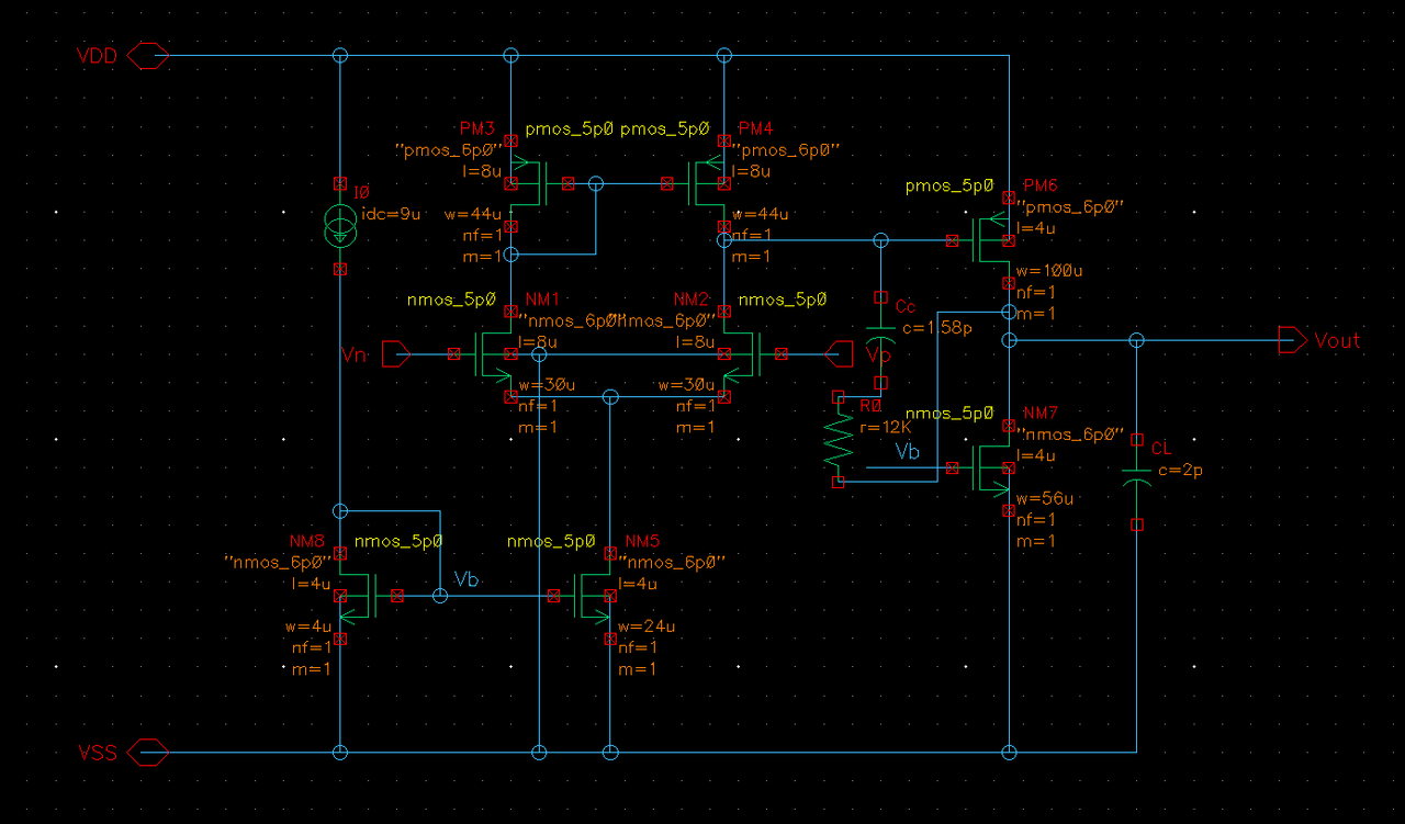
[Figure 1: Schematic of the Two-Stage Miller Compensated OTA]
1.6 Simulation Results (Two-Stage OTA)
DC Operating Point and Power
With and , the total static current is . Total power consumption is roughly , well below the constraint. All critical transistors operate in the deep saturation region.
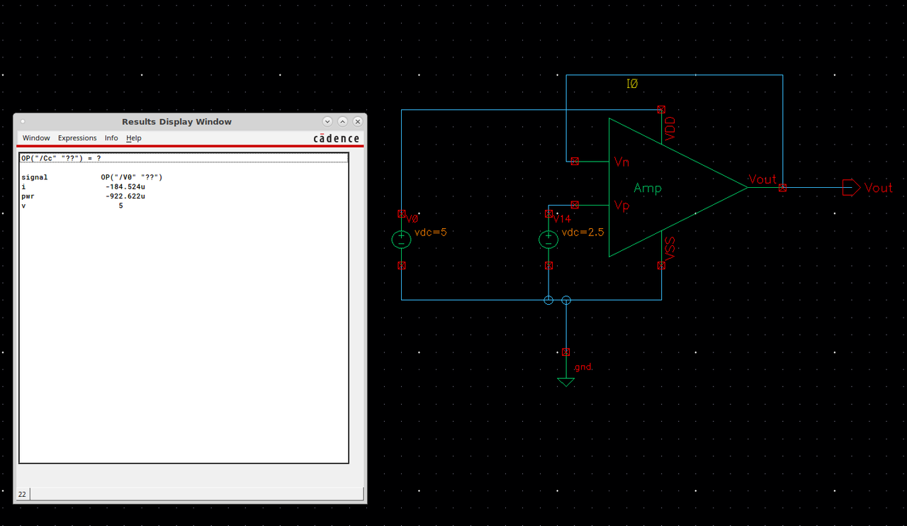
[Figure 2: DC Operating Point of Unity-Gain Buffer]
Stability Analysis (STB)
- DC Loop Gain: 105.24 dB (Exceeds 90dB target due to long-channel devices).
- GBW: 10.94 MHz.
- Phase Margin (PM): . The nulling resistor successfully pushes the RHP zero away, ensuring stability. PM can be read directly on the STB Summary Window.
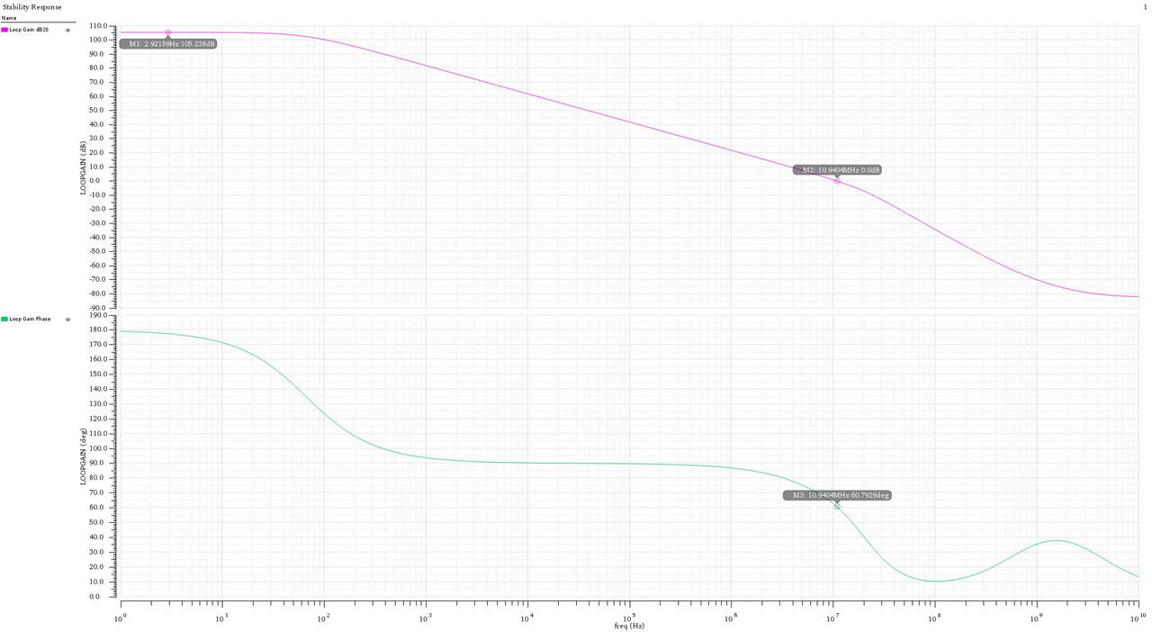
[Figure 3: STB Analysis Amplitude and Phase Plot]
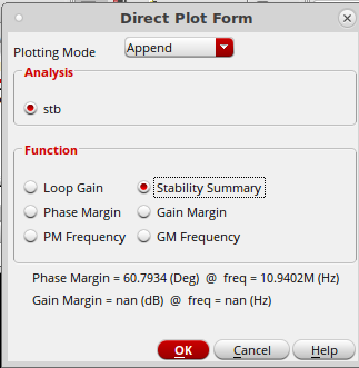
[Figure 4: STB Analysis Summary Window]
AC Analysis (Open-loop and Closed-loop)
When configured as a unity-gain buffer, the closed-loop -3dB bandwidth is measured at 17.15 MHz. Since our system acts as a second-order system with PM , peaking causes the closed-loop -3dB bandwidth to extend beyond the open-loop UGF (theoretically ).
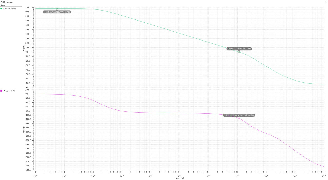
[Figure 5: AC Open Loop Response]
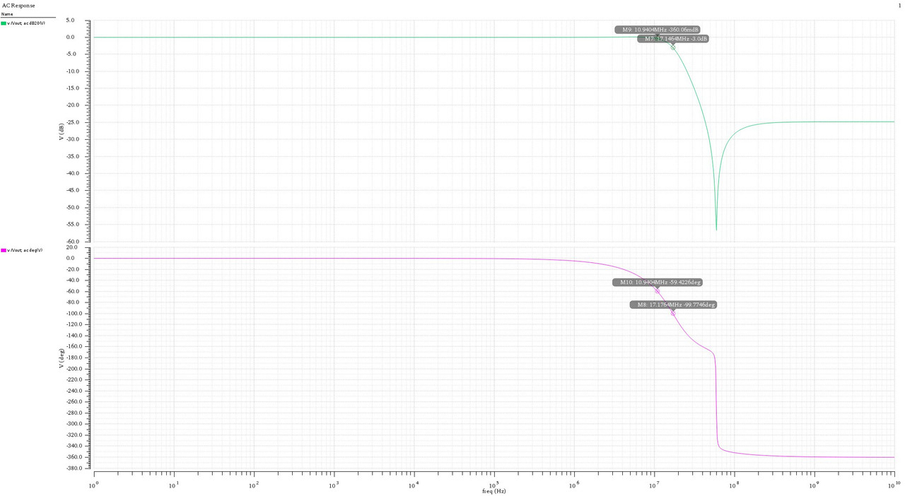
[Figure 6: AC Closed Loop Response]
Transient Response and Slew Rate
Testing with a 250kHz square wave and , the output tracks smoothly without obvious ringing, verifying excellent phase margin.
- Measured SR: (Significantly better than the target).
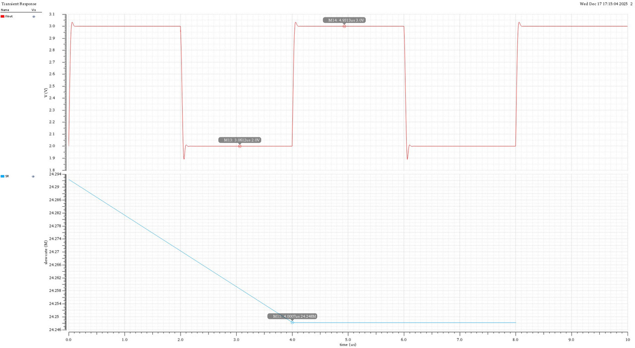
[Figure 7: Transient Analysis and Slew Rate]
Part 2: Two-Stage OTA with a Folded-Cascode First Stage
The second design explores a Folded-Cascode OTA. This topology combines the high-gain characteristics of a cascode stage with the wide input common-mode range of a folded structure.
2.1 Core Topology and Bias Strategy
- Input Stage: We use a PMOS differential pair (PM4, PM5). Signal current flows out of the PMOS drains into the folding nodes.
- Folding Branch & Cascode Load:
- Upper PMOS Cascode: Acts as the main current source and provides extremely high output impedance looking upwards ().
- Lower NMOS Folded Cascode: The signal current is injected into the source of the cascode devices. This matches the upper impedance, guaranteeing massive first-stage gain.
- Bias Network: We employ a Wide-Swing Cascode Bias circuit to generate bias voltages, ensuring maximum output voltage swing.
- Current Distribution: The tail current is set to , split equally ( each) through the input pair. The folding branch is biased at . Therefore, the static current flowing through the lower NMOS cascode stack is . This ensures devices do not turn off during large-signal swings, maintaining a high slew rate. Total power consumption is calculated at .
2.2 Gain and Frequency Compensation
- High Gain Realization: The output impedance at the first stage is the parallel combination of PMOS and NMOS cascode impedances. Even with short channel lengths (), the first-stage gain easily exceeds 60dB. Combined with a second common-source stage, total gain reaches well over 90dB.
- Compensation: We utilize Miller compensation () for pole splitting and a nulling resistor () to boost PM above .
- Slew Rate: Determined by the tail current: .
2.3 Component Sizing Summary (Folded Cascode)
| Module | Component | Type | W () | L () | Function |
|---|---|---|---|---|---|
| Bias Gen | NM0-NM3 | NMOS | 16 | 1 | Wide-swing bias |
| Bias Ref | PM0, PM1 | PMOS | 20 | 2 | Bias reference |
| Tail Current | PM2, PM3 | PMOS | 40 | 2 | tail current |
| Input Pair | PM4, PM5 | PMOS | 100 | 1 | Core transconductance |
| Upper Fold | PM6, PM10 | PMOS | 40 | 2 | Main current source |
| Cascode Up | PM11, PM12 | PMOS | 40 | 2 | Impedance boost |
| Lower Fold | NM4, NM5 | NMOS | 59.025 | 1 | Signal fold / CG stage |
| Current Src | NM6, NM7 | NMOS | 59.025 | 1 | Bottom current source |
| 2nd Stage | NM8 | NMOS | 80 | 1 | CS Amplifier |
| 2nd Stage Ld | PM13 | PMOS | 100 | 2 | Active Load |
| Comp. Net | Cc | Cap | – | – | 1 pF |
| Nulling Res | Rz | Res | – | – | 8 kΩ |
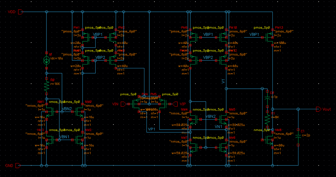
[Figure 8: Schematic of the Folded-Cascode OTA]
2.4 Simulation Results (Folded-Cascode OTA)
DC Analysis
Total current is (Power ). The output DC voltage is naturally stabilized near 2.5V, indicating minimal systematic offset and excellent current mirror matching.
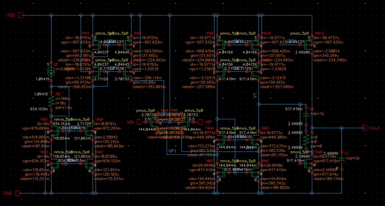
[Figure 9: DC Operating Point of Folded-Cascode OTA]
Stability Analysis (STB)
- DC Loop Gain: 115.1 dB. The cascode structure allows for extreme gain (>110dB) even with short channel lengths, significantly outperforming the standard two-stage OTA.
- GBW: 39.5 MHz. The high transconductance of the input pair () and smaller compensation cap () yield an impressive bandwidth.
- Phase Margin (PM): . An exceptionally safe and optimal value, ensuring smooth transient settling without overshoot.
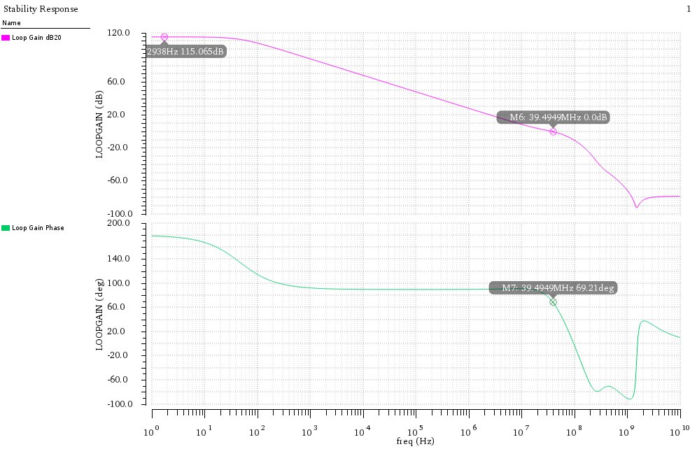
[Figure 10: STB Analysis of Folded-Cascode OTA]
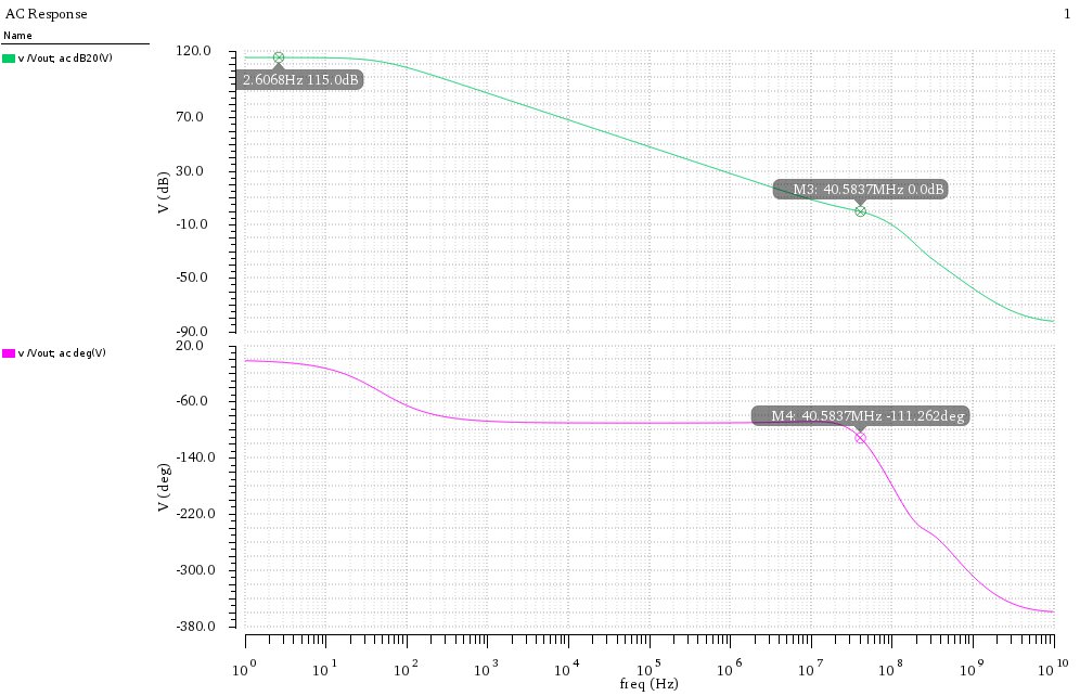
[Figure 11: AC Open Loop Analysis]
AC Closed-Loop Response
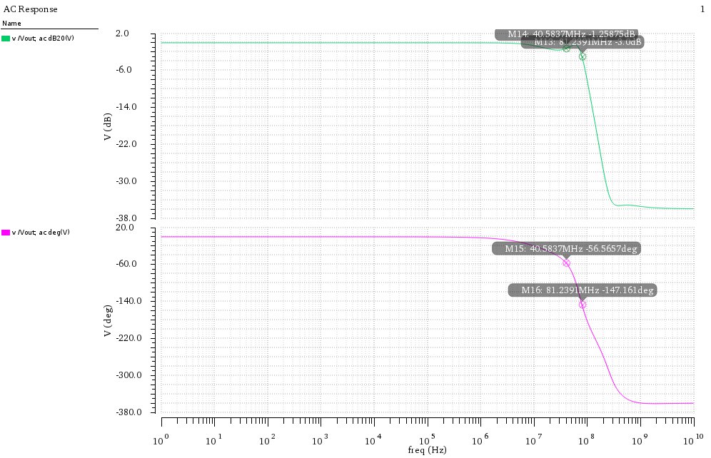
When configured as a unity-gain buffer, the closed-loop -3dB bandwidth stretches to 81.24 MHz (roughly the open-loop UGF). This highlights the superior high-frequency capabilities of the folded-cascode architecture.
Transient Response and Slew Rate
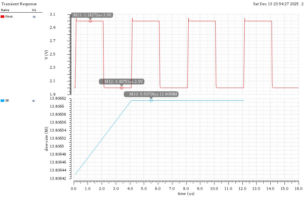
The output perfectly tracks the 250kHz square wave. The rising/falling edges are incredibly clean with zero visible ringing, perfectly reflecting the phase margin.
- Measured SR: .
(Note: The measured SR is slightly lower than the theoretical . This is due to parasitic capacitances at the folding nodes absorbing some charging current, and dynamic shifts in the operating point during large-signal swings. However, is still excellent for a 0.65mW amplifier).
[Figure 12: Transient Analysis and Slew Rate of Folded-Cascode]
Part 3: Deep-Dive Analog Design Concepts
Based on the experiments above, here are three critical concepts every analog designer must master:
3.1 Poles, Zeros, and Pole-Splitting Mechanism
In a two-stage Miller compensated OTA, the small-signal poles are distributed as follows:
- Dominant Pole (p_1): Located at the first-stage output. Due to the Miller effect, is magnified by at this node.
- Non-Dominant Pole (p_2): Located at the second-stage output.
- RHP Zero ($z$): Caused by the feedforward path through .
The Magic of Pole Splitting:
Before adding , the two poles are close together (determined by nodal resistances and parasitics), making the system unstable. Introducing causes a profound effect:
- p_1 moves to a lower frequency (because the effective capacitance at node 1 becomes massive).
- p_2 moves to a higher frequency (because at high frequencies, acts as an AC short circuit between the gate and drain of the second stage, effectively dropping its output resistance to roughly ).
This “one goes low, one goes high” effect splits the poles apart, guaranteeing stability and phase margin.
3.2 What Actually Determines Slew Rate?
Slew rate is the maximum rate of change of the output voltage. It is bottlenecked by the charging/discharging of crucial capacitors ( or ).
- The current available to charge is limited by the first-stage tail current ().
- The current available to charge is limited by the second-stage output current ().
- Design Rule:
In our designs, we ensured the second-stage current was sufficiently large, meaning the SR was primarily limited by the Miller capacitance charging rate.
3.3 Choosing the Right Expression for Design
There are three common ways to express transconductance (g_m):
- (Useful when Bias Current is fixed)
- (Useful when Overdrive Voltage and Linearity are priorities)
- (Useful when Bias Voltage is fixed)
Practical Tip: During layout and circuit sizing, the first formula is often the most practical. Why? Because your total current is usually strictly constrained by the project’s power consumption budget (e.g., <1mW). Under a strict power budget, the most direct way to increase bandwidth (which requires increasing ) is to increase the aspect ratio () of the input transistors.
Conclusion
In this tutorial, we successfully designed two high-gain OTAs:
- The Two-Stage Miller OTA: Achieved an impressive 105 dB open-loop gain by utilizing long-channel devices. With precise and tuning, we secured a phase margin and a Slew Rate, all while staying under 0.93 mW.
- The Two-Stage OTA with a Folded-Cascode First Stage: Demonstrated the power of cascoding by achieving 115 dB gain using short-channel devices (saving layout area). It showcased superior speed with a 39.5 MHz GBW and a closed-loop bandwidth of over 81 MHz, maintaining extreme stability ( PM) at just 0.65 mW.
Both architectures have their unique strengths. Standard two-stage designs are great for high-swing, general-purpose applications, while folded-cascode topologies excel in high-speed, high-gain, and wide common-mode range scenarios.
Leave a Reply