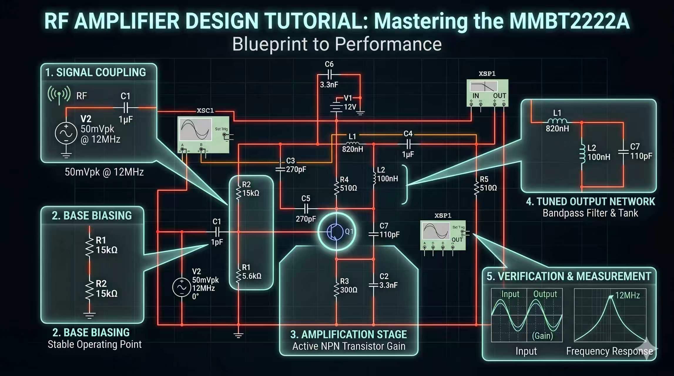

1. Design Scheme
1.1 Design Requirements
Before we start, let’s define the target specifications for our amplifier:
- Transistor: MMBT2222A
- Resonant Frequency (f0): 12 MHz
- Voltage Gain: 25 – 35 dB
- Relative Bandwidth: 25% (Acceptable range: 20% ~ 30%)
- Load Resistance: 510 Ω
- Input Voltage: 50 mV
1.2 Circuit Selection
Based on the requirements, we will use a single-stage amplifier circuit. The collector will feature an LC parallel resonant circuit, making the overall structure equivalent to a single-tuned amplifier.
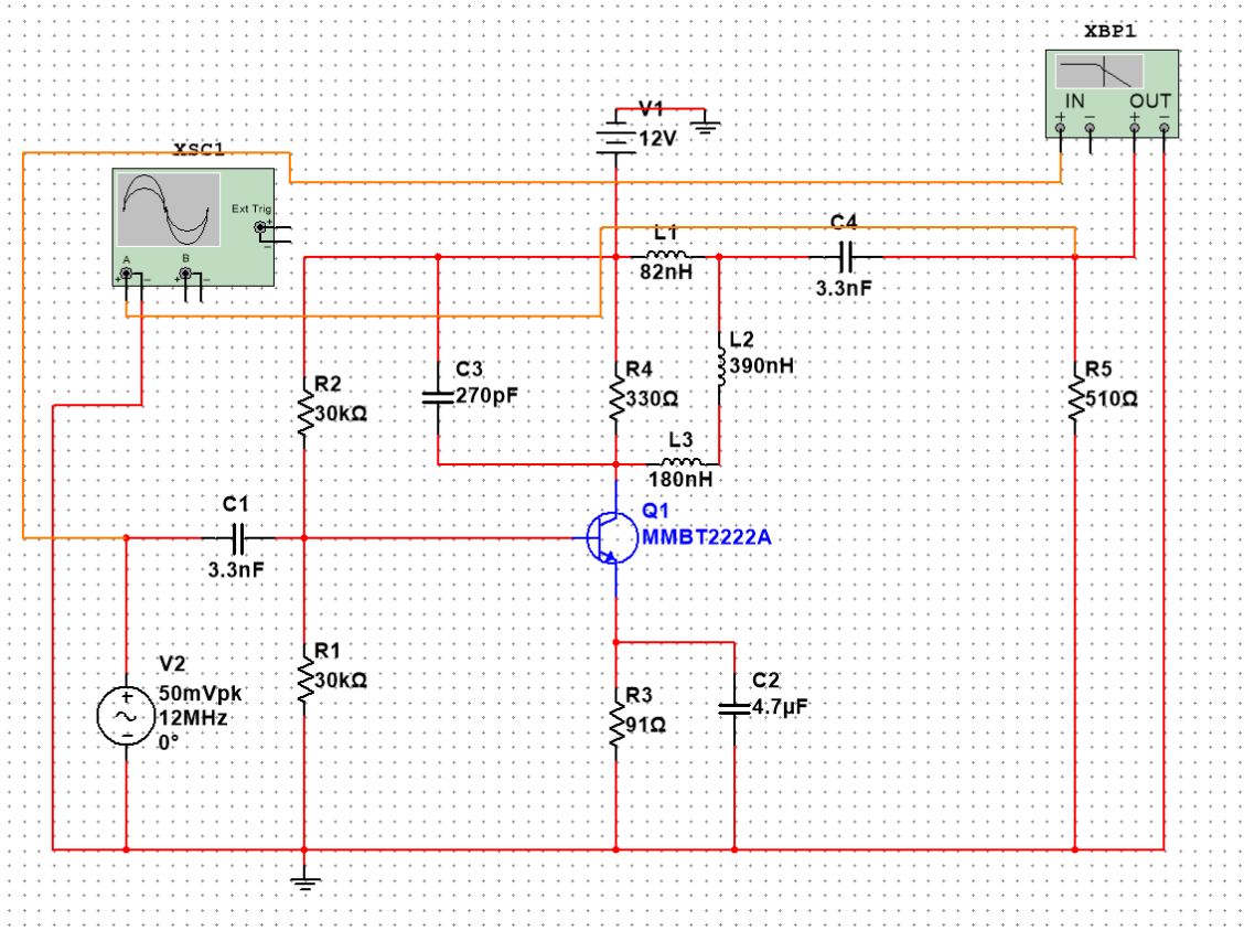
[Figure 1-1: Circuit Schematic Diagram]
2. Parameter Calculation & Component Selection
2.1 Designing the DC Operating Point (Q-Point)
Referring to the MMBT2222A datasheet and the equivalent DC circuit model, we can configure our resistors and bypass capacitor as follows:
- R1 = 5.6 kΩ
- R2 = 15 kΩ
- R3 = 300 Ω
- R4 = 510 Ω
- Bypass Capacitor (C2) = 3.3 nF
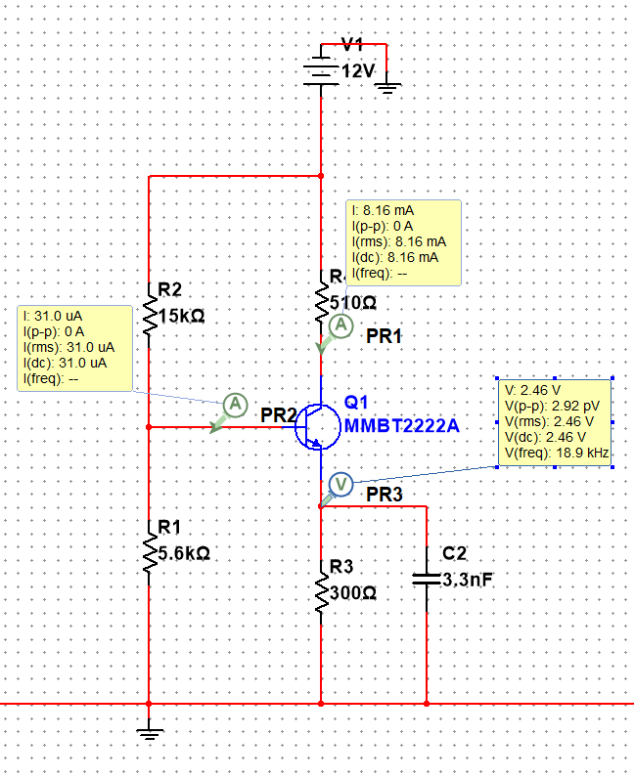
[Figure 2-1: DC Operating Point Test / Simulation]
Based on the test results, our DC characteristics are:
- Base Current (IB) = 31 μA
- Collector Current (IC) = 8.16 mA
- Collector-Emitter Voltage (Uce) = V – Ue = 9.54 V
- With IC = β × IB, we can calculate the current gain β = 263.
These values confirm that the transistor is operating in the active region.
2.2 LC Resonant Circuit Design
To achieve the desired frequency and bandwidth, we use the following formulas:
- Target Center Frequency:
f0 = 1 / (2π√LC) = 12 MHz - Target Bandwidth:
2.4 MHz < B = f0 / QL < 3.6 MHz
Taking the available standard components into consideration, we choose:
- C3 = 180 pF
- L1 = 820 nH
- L2 = 100 nH
Note: Taking the actual transistor parasitic capacitance (approx. 30 pF) into account, the calculated center frequency is f0 = 11.994 MHz, and the bandwidth is B = 2.0 MHz. This perfectly meets our design requirements.
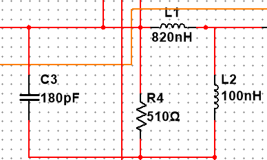
[Figure 2-2: LC Resonant Circuit Diagram]
2.3 Circuit Synthesis
Combining sections 2.1 and 2.2, and adding the output load resistor R5 = 510 Ω along with DC blocking capacitors C1 = C4 = 1 μF, we get our complete circuit.[Insert Image: Figure 2-4 Overall Circuit Diagram]
3. Simulation Debugging and Analysis
3.1 Output Waveform Analysis
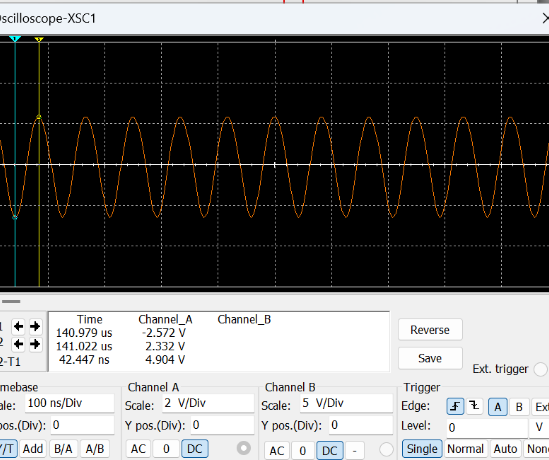
In our simulation software, we input a 12 MHz sine wave with an amplitude of 50 mV. Observing the output on the virtual oscilloscope yields the following waveform:
[Figure 3-1: Output Waveform]
From the graph, the calculated voltage amplification factor is K = 46.6. The output waveform is clean without any distortion, indicating normal operation.
3.2 Bode Plot Analysis
Next, we run an AC sweep to generate the Bode plots.
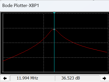
[Figure 3-2: Center Frequency 11.994 MHz]
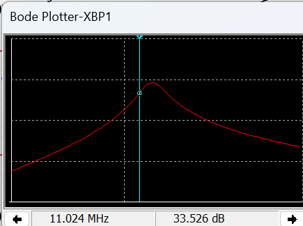
[Figure 3-3: Lower Cutoff Frequency FL = 11.024 MHz]
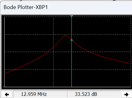
[Figure 3-4: Upper Cutoff Frequency FH = 12.959 MHz]
Simulation Results: The simulated center frequency hits 11.994 MHz with a bandwidth of 1.935 MHz. These values match our theoretical math almost perfectly, confirming that our selected parameters are rock-solid and ready for the physical build!
4. Experimental Verification and Physical Testing
4.1 PCB Fabrication and Soldering
With a successful simulation, we move on to the physical build.
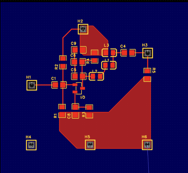
[Figure 4-1: PCB Layout Design]
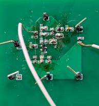
[Figure 4-2: Assembled PCB Board]
4.2 Initial Hardware Test
Using a function generator, we applied a 50 mV sine wave input.
Initial Measurement Results:
- Center Frequency: 9.4 MHz
- Bandwidth: 4 MHz
- Voltage Gain: 25 dB
4.3 Troubleshooting and Correction
There was a noticeable deviation between the hardware test and the simulation—especially regarding the center frequency.
Issue 1: Center Frequency Shift
When testing the physical board, you might notice the center frequency is significantly lower than simulated (e.g., 9.4 MHz instead of 12 MHz). Why does this happen? In the real world, this shift is heavily influenced by the parasitic capacitance of the physical transistor, as well as the hidden capacitance introduced by your oscilloscope probe during measurement!
- Solution: We need to compensate for this extra physical capacitance by reducing the value of C3. By putting two 270 pF capacitors in series, we achieved C3 = 135 pF, which brought the resonant frequency right back to our 12 MHz target.
Issue 2: Lower Voltage Gain & Instability
If your measured gain is lower than expected, it is often a sign of high-frequency noise or an unstable power supply causing partial oscillation.
- Solution: Add a 3.3 nF decoupling/bypass capacitor between Vcc and GND. Make sure to place it as close to the transistor’s circuit as possible. This simple trick cleans up the power supply and helps the amplifier achieve its full 35 dB gain.
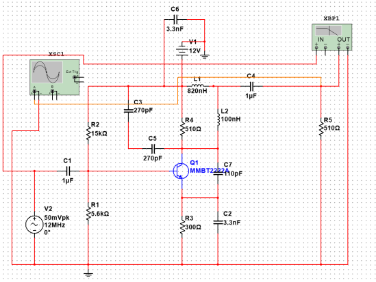
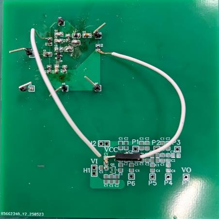
[Figure 4-3: Modified Circuit schematic / Physical setup]
4.4 Final Assessment Test
After making the modifications, we tested the circuit again:
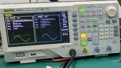
[Figure 4-4: Final Amplified Signal on Oscilloscope]
Final Measurement Results:
- Center Frequency: 11.95 MHz
- Bandwidth: 3.7 MHz
- Voltage Gain: 35 dB
5. Conclusion and Key Takeaways
Congratulations on successfully designing, simulating, and building your own high-frequency small-signal resonant amplifier!
In this tutorial, we walked through the complete hardware engineering workflow:
- Theoretical Calculation: Setting up a stable DC operating point and calculating the LC tank parameters for the target frequency.
- Circuit Simulation: Verifying our math and observing the ideal AC responses and Bode plots.
- Hardware Troubleshooting: Bridging the gap between software simulation and physical reality.
The most valuable lesson here is understanding that real-world components are never ideal. As we saw during the physical hardware test, the center frequency shifted and the gain was initially unstable. This perfectly illustrates the hidden impact of parasitic parameters—such as the transistor’s internal junction capacitance, PCB trace inductance, and even the capacitance introduced by your oscilloscope probes!
Learning how to systematically identify these physical variables and compensate for them (like tuning C3 and adding bypass capacitors) is exactly what turns a theoretical concept into a robust, working circuit.
We hope this guide has given you the hands-on confidence to tackle more advanced RF and high-frequency circuit designs. Happy building!
Leave a Reply